Lattice公司的LatticeECP3 Versa評估板" title="評估板">評估板使設(shè)計(jì)者能評價和實(shí)驗(yàn)LatticeECP3現(xiàn)場可編門陣列,而LatticeECP3系列可提供高性能的特性如增強(qiáng)DSP架構(gòu),高速SERDES和FPGA中高速源同步接口,這些特性使得LatticeECP3系列非常適合用在量大高速低成本的產(chǎn)品如工業(yè)網(wǎng)絡(luò)" title="工業(yè)網(wǎng)絡(luò)">工業(yè)網(wǎng)絡(luò),工廠自動化" title="工廠自動化">工廠自動化,計(jì)算,醫(yī)療設(shè)備,國防和消費(fèi)類電子" title="消費(fèi)類電子">消費(fèi)類電子.本文介紹了LatticeECP3主要特性" title="主要特性">主要特性, LatticeECP3-35簡化方框圖和LatticeECP3 Versa 評估板主要特性,方框圖,電路圖,材料清單和元件布局圖.
The LatticeECP3™ (EConomy Plus Third generation) family of FPGA devices is optimized to deliver high performance features such as an enhanced DSP architecture, high speed SERDES and high speed source synchronous interfaces in an economical FPGA fabric. This combination is achieved through advances in device architecture and the use of 65nm technology making the devices suitable for high-volume, high-speed, low-cost applications. The LatticeECP3 device family expands look-up-table (LUT) capacity to 149K logic elements and supports up to 586 user I/Os. The LatticeECP3 device family also offers up to 320 18x18 multipliers and a wide range of parallel I/O standards. The LatticeECP3 FPGA fabric is optimized with high performance and low cost in mind. The LatticeECP3 devices utilize reconfigurable SRAM logic technology and provide popular building blocks such as LUT-based logic, distrib-uted and embedded memory, Phase Locked Loops (PLLs), Delay Locked Loops (DLLs), pre-engineered source synchronous I/O support, enhanced sysDSP slices and advanced configuration support, including encryption and dual-boot capabilities. The pre-engineered source synchronous logic implemented in the LatticeECP3 device family supports a broad range of interface standards, including DDR3, XGMII and 7:1 LVDS. The LatticeECP3 device family also features high speed SERDES with dedicated PCS functions. High jitter toler-ance and low transmit jitter allow the SERDES plus PCS blocks to be configured to support an array of popular data protocols including PCI Express, SMPTE, Ethernet (XAUI, GbE, and SGMII) and CPRI. Transmit Pre-empha-sis and Receive Equalization settings make the SERDES suitable for transmission and reception over various forms of media. The LatticeECP3 devices also provide flexible, reliable and secure configuration options, such as dual-boot capa-bility, bit-stream encryption, and TransFR field upgrade features. The Lattice Diamond™ and ispLEVER® design software allows large complex designs to be efficiently imple-mented using the LatticeECP3 FPGA family. Synthesis library support for LatticeECP3 is available for popular logic synthesis tools. Diamond and ispLEVER tools use the synthesis tool output along with the constraints from its floor planning tools to place and route the design in the LatticeECP3 device. The tools extract the timing from the routing and back-annotate it into the design for timing verification. Lattice provides many pre-engineered IP (Intellectual Property) modules for the LatticeECP3 family. By using these configurable soft core IPs as standardized blocks, designers are free to concentrate on the unique aspects of their design, increasing their productivity.
Each LatticeECP3 device contains an array of logic blocks surrounded by Programmable I/O Cells (PIC). Interspersed between the rows of logic blocks are rows of sysMEM™ Embedded Block RAM (EBR) and rows of sys- DSP™ Digital Signal Processing slices, as shown in Figure 2-1. The LatticeECP3-150 has four rows of DSP slices; all other LatticeECP3 devices have two rows of DSP slices. In addition, the LatticeECP3 family contains SERDES Quads on the bottom of the device. There are two kinds of logic blocks, the Programmable Functional Unit (PFU) and Programmable Functional Unit without RAM (PFF). The PFU contains the building blocks for logic, arithmetic, RAM and ROM functions. The PFF block contains building blocks for logic, arithmetic and ROM functions. Both PFU and PFF blocks are optimized for flexibility, allowing complex designs to be implemented quickly and efficiently. Logic Blocks are arranged in a twodimensional array. Only one type of block is used per row. The LatticeECP3 devices contain one or more rows of sysMEM EBR blocks. sysMEM EBRs are large, dedicated 18Kbit fast memory blocks. Each sysMEM block can be configured in a variety of depths and widths as RAM or ROM. In addition, LatticeECP3 devices contain up to two rows of DSP slices. Each DSP slice has multipliers and adder/accumulators, which are the building blocks for complex signal processing capabilities. The LatticeECP3 devices feature up to 16 embedded 3.2Gbps SERDES (Serializer / Deserializer) channels. Each SERDES channel contains independent 8b/10b encoding / decoding, polarity adjust and elastic buffer logic. Each group of four SERDES channels, along with its Physical Coding Sub-layer (PCS) block, creates a quad. The functionality of the SERDES/PCS quads can be controlled by memory cells set during device configuration or by registers that are addressable during device operation. The registers in every quad can be programmed via the SERDES Client Interface (SCI). These quads (up to four) are located at the bottom of the devices. Each PIC block encompasses two PIOs (PIO pairs) with their respective sysI/O buffers. The sysI/O buffers of the LatticeECP3 devices are arranged in seven banks, allowing the implementation of a wide variety of I/O standards. In addition, a separate I/O bank is provided for the programming interfaces. 50% of the PIO pairs on the left and right edges of the device can be configured as LVDS transmit/receive pairs. The PIC logic also includes pre-engineered support to aid in the implementation of high speed source synchronous standards such as XGMII, 7:1 LVDS, along with memory interfaces including DDR3. Other blocks provided include PLLs, DLLs and configuration functions. The LatticeECP3 architecture provides two Delay Locked Loops (DLLs) and up to ten Phase Locked Loops (PLLs). The PLL and DLL blocks are located at the end of the EBR/DSP rows. The configuration block that supports features such as configuration bit-stream decryption, transparent updates and dual-boot support is located toward the center of this EBR row. Every device in the LatticeECP3 family supports a sysCONFIG™ port located in the corner between banks one and two, which allows for serial or parallel device configuration. In addition, every device in the family has a JTAG port. This family also provides an on-chip oscillator and soft error detect capability. The LatticeECP3 devices use 1.2V as their core voltage.
LatticeECP3主要特性:
Higher Logic Density for Increased System Integration
• 17K to 149K LUTs
• 133 to 586 I/Os
Embedded SERDES
• 150 Mbps to 3.2 Gbps for Generic 8b10b, 10-bit SERDES, and 8-bit SERDES modes
• Data Rates 230 Mbps to 3.2 Gbps per channel for all other protocols
• Up to 16 channels per device: PCI Express, SONET/SDH, Ethernet (1GbE, SGMII, XAUI), CPRI, SMPTE 3G and Serial RapidIO
sysDSP™
• Fully cascadable slice architecture
• 12 to 160 slices for high performance multiply and accumulate
• Powerful 54-bit ALU operations
• Time Division Multiplexing MAC Sharing
• Rounding and truncation
• Each slice supports
–Half 36x36, two 18x18 or four 9x9 multipliers
–Advanced 18x36 MAC and 18x18 Multiply-Multiply-Accumulate (MMAC) operations
Flexible Memory Resources
• Up to 6.85Mbits sysMEM™ Embedded Block RAM (EBR)
• 36K to 303K bits distributed RAM
sysCLOCK Analog PLLs and DLLs
• Two DLLs and up to ten PLLs per device
Pre-Engineered Source Synchronous I/O
• DDR registers in I/O cells
• Dedicated read/write levelling functionality
• Dedicated gearing logic
• Source synchronous standards support
–ADC/DAC, 7:1 LVDS, XGMII
–High Speed ADC/DAC devices
• Dedicated DDR/DDR2/DDR3 memory with DQS support
• Optional Inter-Symbol Interference (ISI) ? correction on outputs
Programmable sysI/O™ Buffer Supports Wide Range of Interfaces
• On-chip termination
• Optional equalization filter on inputs
• LVTTL and LVCMOS 33/25/18/15/12
• SSTL 33/25/18/15 I, II
• HSTL15 I and HSTL18 I, II
• PCI and Differential HSTL, SSTL
• LVDS, Bus-LVDS, LVPECL, RSDS, MLVDS
Flexible Device Configuration
• Dedicated bank for configuration I/Os
• SPI boot flash interface
• Dual-boot images supported
• Slave SPI
• TransFR™ I/O for simple field updates
• Soft Error Detect embedded macro
System Level Support
• IEEE 1149.1 and IEEE 1532 compliant
• Reveal Logic Analyzer
• ORCAstra FPGA configuration utility
• On-chip oscillator for initialization & general use
• 1.2V core power supply
LatticeECP3系列產(chǎn)品選擇表:


圖1.LatticeECP3-35簡化方框圖(頂視圖)
LatticeECP3 Versa 評估板
The LatticeECP3™ Versa Evaluation Board allows designers to investigate and experiment with the features of the LatticeECP3 Field-Programmable Gate Array. The features of the LatticeECP3 Versa Evaluation Board can assist engineers with rapid prototyping and testing of their specific designs. The LatticeECP3 Versa Evaluation Board is part of the LatticeECP3 Versa Development Kit. The guide is intended to be referenced in conjunction with demo user’s guides to demonstrate the LatticeECP3 FPGA.

圖2.LatticeECP3 Versa 評估板外形圖
LatticeECP3 Versa 評估板主要特性:
• Half-length PCI Express form-factor
– Allows demonstration of PCI Express x1 interconnection
• Electrical testing of one full-duplex SERDES channel via SMA connections
• USB-B connection for UART and device programming
• Two RJ45 interfaces to 10/100/1000 Ethernet to GMII
• On-board Boot Flash – 64M Serial SPI Flash
• DDR3-1333 memory components (64Mb/x16)
• Expansion mezzanine interconnection for prototyping
• 14-segment alpha-numeric display
• Switches, LEDs and displays for demo purposes
• ispVM™ programming support
• On-board reference clock sources
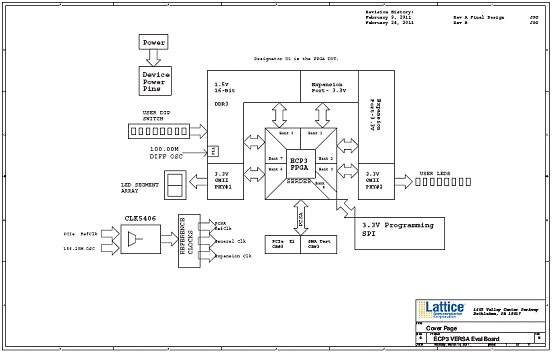
圖3.LatticeECP3 Versa評估板方框圖
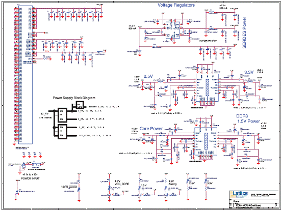
圖4.LatticeECP3 Versa評估板電路圖(1)

圖5.LatticeECP3 Versa評估板電路圖(2)

圖6.LatticeECP3 Versa評估板電路圖(3)

圖7.LatticeECP3 Versa評估板電路圖(4)
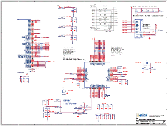
圖8.LatticeECP3 Versa評估板電路圖(5)
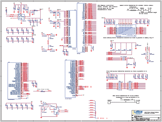
圖9.LatticeECP3 Versa評估板電路圖(6)

圖10.LatticeECP3 Versa評估板電路圖(7)
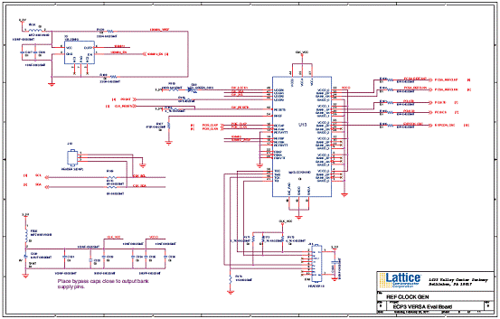
圖11.LatticeECP3 Versa評估板電路圖(8)

圖12LatticeECP3 Versa評估板電路圖(9)
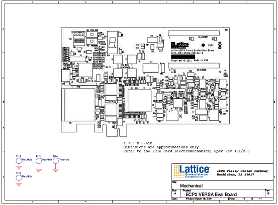
圖13.LatticeECP3 Versa評估板元件布局圖
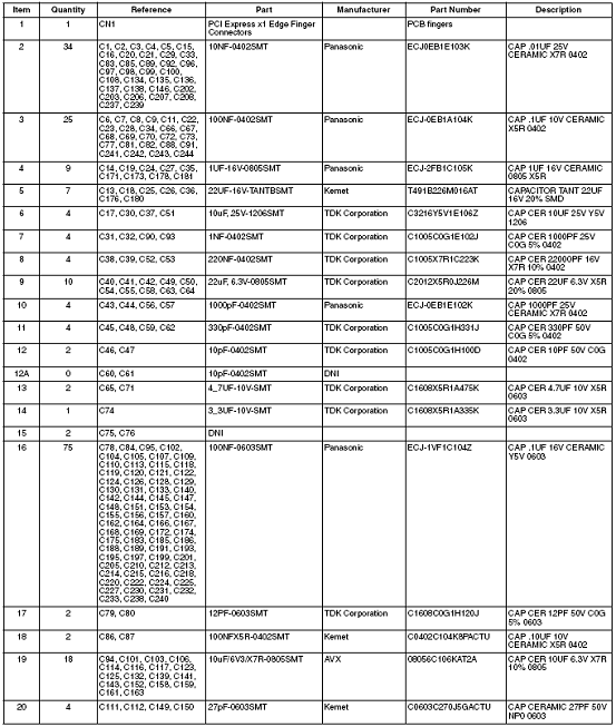
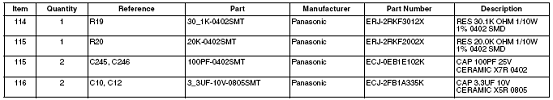
LatticeECP3 Versa評估板材料清單(BOM):


詳情請見:
http://www.latticesemi.com/documents/ds1021ea.pdf
和
http://www.latticesemi.com/documents/EB62.pdf
